Renaissance Solar and Electronic Materials (RSOLEC), a solar enterprise with operations in India and the USA, has announced its venture for solar crystal growth and wafering in India. The company plans to expand its presence across the entire solar value chain eventually.
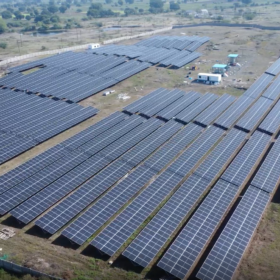
RSOLEC will initially set up a solar crystal growth and wafering facility with a production capacity of 5 GW per annum and plans expansion to exceed 20 GW in the long term. Commissioning of the facility is planned in late 2025 and production is set to start in 2026.
RSOLEC is currently evaluating several short-listed production sites offering attractive opportunities.
The company announced its solar manufacturing plans for India following its official launch and establishment, accompanied by a planned investment of about $300 million recently.
“With global reach and expertise in differentiated solar and electronic materials manufacturing, RSOLEC is set to revolutionize the industry with a strategic focus on solar crystal growth and wafering,” announced the company.
RSOLEC stated its primary focus for the next five years will be on crystal growth and wafering in India, contributing significantly to the country’s strategic solar manufacturing capacity. Over the long term, the company will expand its manufacturing over the entire solar value chain.
RSOLEC aims to pioneer solar manufacturing with the lowest capital intensity, ensuring cost-competitive production on a global scale. The company’s roadmap anticipates achieving a capital intensity below $35 million per GW.
Technology
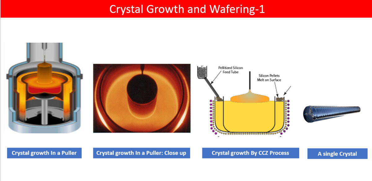
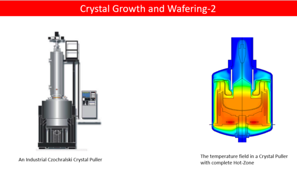
RSOLEC stated its facility will utilize the state-of-the-art Recharge Czochralski (RCZ) process, which can be retrofitted to the emerging Continuous Czochralski (CCZ) process for crystal growth. Wafer production will be based on the cutting-edge DCW platform, capable of producing thin wafers measuring below 100 micrometers in thickness.
The primary product will be high-quality silicon wafers with low oxygen content, long lifetime, and controlled resistivity. These will be compatible with all solar cell technologies, including TOPCon, PERC, HJT, and Tandem structures.
RSOLEC aims to achieve crystals with uniform resistivity, potentially increasing average cell efficiency by 0.15%, a milestone not yet attained in the solar manufacturing industry. For select customers requiring very low oxygen content, the magnetic Czochralski (MCZ) platform will be employed. The facility will have the capability to produce wafers in various sizes, including M10, G12, and G16.

The company claims to achieve an 80% improvement in productivity and a 40% reduction in production costs over a short timeframe by leveraging its continuous technological advancement on existing platforms.
RSOLEC is founded and supported by technocrats from five different countries across three continents. The company is based in Delaware, USA, and operates through its Indian subsidiary located within the IIT Madras Research Park.
Milind Kulkarni, chairman and CEO of RSOLEC, articulated, “RSOLEC is poised to contribute to the solar energy revolution and initiate the cultural transformation required for success in the dynamic solar manufacturing sector. Our differentiation lies in our technology-driven, low-risk innovations, positioning RSOLEC at the forefront of the solar industry.”
“It is strategically imperative for India to develop the entire solar ecosystem, encompassing solar manufacturing. RSOLEC brings the requisite expertise for technology-driven solar manufacturing, and we are pleased to support this critically significant endeavor at the IIT Madras Research Park,” added Ashok Jhunjhunwala, President of IITM Research Park.
This content is protected by copyright and may not be reused. If you want to cooperate with us and would like to reuse some of our content, please contact: editors@pv-magazine.com.


By submitting this form you agree to pv magazine using your data for the purposes of publishing your comment.
Your personal data will only be disclosed or otherwise transmitted to third parties for the purposes of spam filtering or if this is necessary for technical maintenance of the website. Any other transfer to third parties will not take place unless this is justified on the basis of applicable data protection regulations or if pv magazine is legally obliged to do so.
You may revoke this consent at any time with effect for the future, in which case your personal data will be deleted immediately. Otherwise, your data will be deleted if pv magazine has processed your request or the purpose of data storage is fulfilled.
Further information on data privacy can be found in our Data Protection Policy.