From pv magazine USA
Ten scientists have projected the innovation pathways for the major PV cell technologies over the next five years, in an open-access article in the journal Cell.
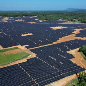
Although installed PV capacity worldwide exceeds 1 terawatt (1,000 GW), PV’s contribution to worldwide electricity generation remains small, the authors say, at 5% to 6%. Given an “urgent need” to deploy PV at multi-terawatt (TW) scale over the next two decades to mitigate greenhouse gas emissions, “PV device innovation takes on new urgency and impact.”
Continued research that leads to “even relatively small advances” in efficiency, reliability and manufacturing efficiency “will have major future impacts at multi-TW scale,” the authors say, as these factors combine to make “the increasingly compelling value proposition” for PV power generation.
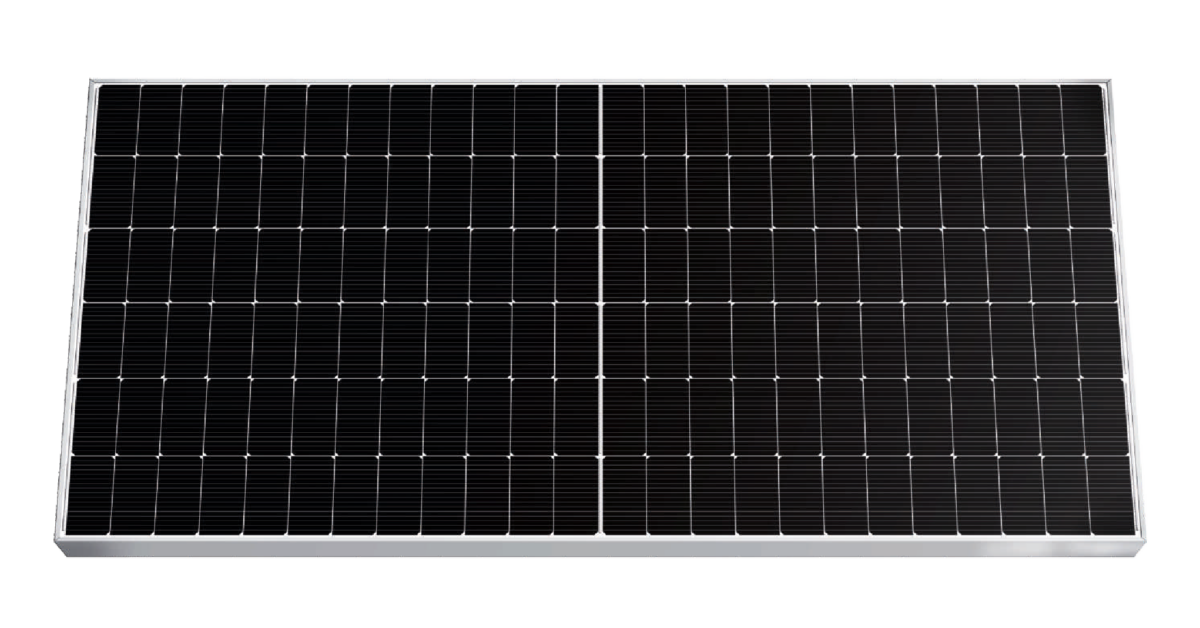
While crystalline silicon PV had a 95% market share in 2022, in a “TW-scale future” with “PV everywhere,” multiple technologies may be complementary, or combined, the authors say.
The silicon PV technology known as TOPCon (tunnel oxide passivating contact), with a market share of 23%, will “overcome” production of PERC (passivated emitter and rear cell) PV by 2025 and “is likely to become the technology of choice for new-cell manufacturing in the US,” the article predicts.
Crystalline silicon PV cells are approaching the single-junction theoretical maximum efficiency of 29.4%, the authors say.
Research is still needed, they note, to develop high-temperature, selective area passivating contacts on both sides of the PV cell (“advanced TOPCon”), to improve the transparency and conductivity of heterojunction technology (HJT) contacts (“advanced HJT”), and to combine the latest HJT or TOPCon technologies with an interdigitated back contact (IBC) structure, “which could reach an ultimate practical efficiency of 28% possibly as soon as 2025.”
Yet as the theoretical limit is approached, “several new modes of degradation, called carrier-induced degradation, and metastable defects are unveiled,” the authors say.
The industry “is working to reduce or eliminate” the use of scarce materials such as silver for the formation of grid lines and indium used in transparent conductive oxides, the authors say. Several PV companies and research laboratories have announced HJT PV cell design with reduced indium consumption “or even indium-free” HJT cells.
Tandem technology
Many technologies for tandem solar cells have been proposed to overcome the single-junction efficiency limit, the authors say.
Development of monolithic 2-terminal perovskite/silicon tandem cells, “considered by many as the most probable and cost-effective solution,” is currently the most active research area, and has already yielded a record cell efficiency of 33.7% for a small-area (1 square centimeter) cell.
For a 30% efficient 2-terminal tandem cell, “the efficiency of the top cell is significantly more critical than the efficiency of the bottom cell,” so “a potential contender as a bottom cell” would include “almost any” silicon cell technology.
While “there is no doubt” that efficiencies greater than 30% will soon be commercially available on large-area cells, “stability still needs to be improved,” the authors say. To reach the same levelized cost of electricity (LCOE) as established “bankable” technologies, “the tandem device may only degrade less than 0.5% per year.”
Cadmium telluride
Cadmium telluride (CdTe) PV technology accounts for 25% of installed U.S. utility-scale PV, but only 5% of global market share. The researchers projected, based on a First Solar cell with arsenic-doped material that reached 22.3% efficiency, that Cd(Se,Te) cells doped with a Group V material “will become the primary platform for research, development and manufacturing.”
CIGS
Turning to CIGS technology, whose original formulation used copper, indium, gallium and selenium, the authors say that the combination of CIGS in tandem applications is “one major focus of future developments.” CIGS tandem devices “are not limited to pairing CIGS with perovskites,” they add, as “they may be made with numerous materials including CdTe-, Si-, or CIGS-based alloys with different band gaps.”
Multi-junction III-V
Multi-junction III-V PV cells are described by the U.S. Department of Energy as cells that can reach efficiencies over 45% by using multiple bandgaps, or junctions, that are each tuned to absorb a specific region of the solar spectrum. Multi-junction III-V PV cells could enable “significant space-based power generation,” the authors say.
The article, written by five scientists from the U.S. National Renewable Energy Laboratory and five others from First Solar and research institutes in Germany, the U.S. and China, is titled “Photovoltaic device innovation for a solar future.”
Three of the co-authors contributed to an article in the journal Science earlier this year titled “Photovoltaics at multi-terawatt scale: Waiting is not an option.”
This content is protected by copyright and may not be reused. If you want to cooperate with us and would like to reuse some of our content, please contact: editors@pv-magazine.com.


By submitting this form you agree to pv magazine using your data for the purposes of publishing your comment.
Your personal data will only be disclosed or otherwise transmitted to third parties for the purposes of spam filtering or if this is necessary for technical maintenance of the website. Any other transfer to third parties will not take place unless this is justified on the basis of applicable data protection regulations or if pv magazine is legally obliged to do so.
You may revoke this consent at any time with effect for the future, in which case your personal data will be deleted immediately. Otherwise, your data will be deleted if pv magazine has processed your request or the purpose of data storage is fulfilled.
Further information on data privacy can be found in our Data Protection Policy.