From pv magazine 07-08/23
Cost reduction and efficiency improvement are the shared pursuits of the PV industry, with the former of vital importance in the wafer sector. Manufacturers strive to seek the best wafer thickness and format, leading to the current technology roadmaps for fabricating thinner and larger wafers.
With tier-1 manufacturers taking the lead, the mainstream thickness of positively-doped, p-type wafers now sits at 150 microns and the typical thickness of n-type wafers is 130 microns.
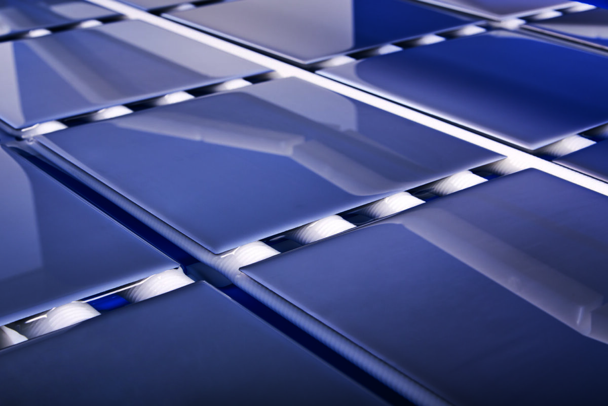
While wafer thickness appears to be gradually unifying, wafer size and shape is a different story. Between 2013 and 2017, 156 mm “M0” and 156.75 mm “M2” wafers dominated the market upon the emergence of aluminum back surface field solar cell technology.
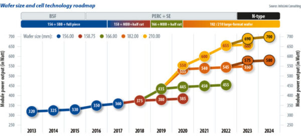
In 2018, the switch to mono PERC (passivated emitter rear contact) technology began a fast-changing wafer-format landscape as manufacturers sought cost optimization. By 2019 and 2020, there were numerous formats available on the market. Today, M6 (166 mm), M10 (182 mm), and G12 (210 mm) wafers account for appreciable market shares, with the latter two the most widely adopted.
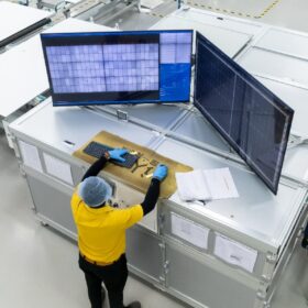
When large-format wafers were still nascent, module makers did not reach a consensus on module specs, posing more problems to their raw material suppliers. In September 2021, Longi, Jinko, and JA Solar came to an agreement for modules based on 182 mm cells, with 72-cell, 2,278 mm by 1,134 mm being the most mainstream spec, ramping up the unification of module design across the industry.
Size advantages
Increasing wafer area improves module efficiency and reduces balance of system (BOS) costs and the overall levelized cost of energy for solar. Initially, vertically integrated companies with wafer production capacity adjusted wafer formats to achieve the highest module output. For instance, Longi introduced 182 mm by 183.75 mm wafers using triangle ribbon and flat ribbon segmentation, and JA Solar launched 182 mm by 185.3 mm pieces using gapless flexible interconnection technology. Henceforth, the combination of “rectangular wafers” and “high-density encapsulation” became a focus of the industry for future development.
Having attempted to make the most use of module area while keeping the module spec of 2,278 mm by 1,134 mm, module makers came to realize that the original format did not fully utilize shipping containers. They adjusted the length of modules as a result, coming up with varying specs to accommodate larger wafers.
Module makers kept the width at 1,134 mm to stack two arrays of pallets in a 40 ft shipping container without exceeding the door opening height. In addition to the original spec of 2,278 mm for modules with a higher cell count, manufacturers also innovated while keeping the length within 2,386 mm, in order to house 20 pallets in a 40-foot cube container. Considering EU structural design standards the “Eurocodes,” some tried to keep the length of modules with smaller cell counts within 2 m.
Diversity reigns
The resulting myriad of wafer formats brings chaos and inconvenience to the PV industry. Non-vertically integrated companies selling or buying customized wafers are having a hard time. Wafer makers have to negotiate orders for rectangular wafers in each format, while cell and module makers struggle to sell leftover customized products. Adjusting fixers or encapsulant, glass, and other components pushes up costs, testing the supply chain management ability of manufacturers.
End users must track the changes of module specs because such diversification complicates system design and management. Once module specs change, customers have to adjust their BOS equipment accordingly, including the distance between mounting holes, the tracking systems, and inverters. Dispatching solar module supply also becomes more difficult for them.
Despite the heterogeneity, and the absence of an official announcement from any module maker, this year’s SNEC and Intersolar Europe trade shows featured modules from leading manufacturers comprised of rectangular wafers that displayed a smaller disparity in specs.
The length of 45-cell and 48-cell modules still varied between 1,722 mm, 1,762 mm, and 1,780 mm, however. As for 66-cell and 72-cell modules, in addition to the regular 2,278 mm by 1,134 mm, there was also a gain in popularity for 2,380-something mm by 1,134 mm devices. In mid-June, nine manufacturers were reportedly on board for unified module specs, paving the way for the future standardization of modules.
About the author: Alan Tu is an assistant analyst with InfoLink Consulting’s solar research team. He focuses on solar demand and national policies, monitoring the changing policy trajectory, and potential PV industry impacts.
The views and opinions expressed in this article are the author’s own, and do not necessarily reflect those held by pv magazine.
This content is protected by copyright and may not be reused. If you want to cooperate with us and would like to reuse some of our content, please contact: editors@pv-magazine.com.


By submitting this form you agree to pv magazine using your data for the purposes of publishing your comment.
Your personal data will only be disclosed or otherwise transmitted to third parties for the purposes of spam filtering or if this is necessary for technical maintenance of the website. Any other transfer to third parties will not take place unless this is justified on the basis of applicable data protection regulations or if pv magazine is legally obliged to do so.
You may revoke this consent at any time with effect for the future, in which case your personal data will be deleted immediately. Otherwise, your data will be deleted if pv magazine has processed your request or the purpose of data storage is fulfilled.
Further information on data privacy can be found in our Data Protection Policy.