From pv magazine International
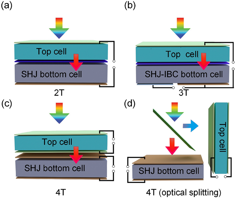
In a paper published in the journal Nanophotonics, scientists at Nankai University provide an overview of current research on silicon heterojunction tandem solar cells (SHJ-TSCs), including perovskite/SHJ TSCs and III–V/SHJ TSCs, and highlight the opportunities and challenges of this technology.
According to their analysis, the big challenge for perovskite/SHJ TSCs is the open-circuit voltage (Voc ) loss, which is mainly caused by nonradiative recombination at the grain boundary and interface. To address this issue, a range of strategies have been applied to date including increasing grain size, surface passivation, 2D/3D heterojunction engineering, and ion compensation.
However, defects passivation has emerged as the most powerful means to improve Voc. A lot of research effort is currently focused on Lewis bases/acids, alkali metal ions (Na, K, Ru, Cs), ligand passivation, halogen ion (Cl, Br), PbI2, 2D perovskite, insulating polymers, and guanidinium-based additives, the review finds.
Another issue is fabricating perovskite top cells on textured c-Si cells, where the vacuum deposition method can yield good results, according to the study.
“To further improve the TSCs performance, optical and electron losses have to be minimized. If these issues are solved, a power conversion efficiency (PCE) over 35% can be expected,” the review reads. For up-scaling fabrication and commercialization, long-term stability and material toxicity are also needed to be optimized, said the Chinese scientists.
III–V
Unlike perovskites, III–V compound semiconductor materials, with their proven reliability and adjustable bandgap, exhibit high efficiency and promising potential for industrial application. However, they are plagued by high costs.
So far, many strategies have been used to fabricate III–V/SHJ TSCs, including heteroepitaxial growth, wafer bonding, and mechanical stacking. The heteroepitaxial integration approach based on the control of dislocation densities at the interface has been used to produce devices, but their quality was poor. Approaches based on surface activated bonding (SAB) seem to be most versatile in fabricating high efficiency III–V/SHJ TSCs. This method, however, is not appropriate for use with textured SHJ solar cells, and the requirement of a cleanroom environment and tunnel junction may also cause high cost.
Therefore, mechanical stacking by transparent conductive adhesive and metal nanoparticle array may be a new research direction for high-performance III–V/SHJ TSCs, the review states. However, it concludes that all the approaches described need to be improved in terms of performance and cost before they can be widely used in commercial applications.
This content is protected by copyright and may not be reused. If you want to cooperate with us and would like to reuse some of our content, please contact: editors@pv-magazine.com.


2 comments
By submitting this form you agree to pv magazine using your data for the purposes of publishing your comment.
Your personal data will only be disclosed or otherwise transmitted to third parties for the purposes of spam filtering or if this is necessary for technical maintenance of the website. Any other transfer to third parties will not take place unless this is justified on the basis of applicable data protection regulations or if pv magazine is legally obliged to do so.
You may revoke this consent at any time with effect for the future, in which case your personal data will be deleted immediately. Otherwise, your data will be deleted if pv magazine has processed your request or the purpose of data storage is fulfilled.
Further information on data privacy can be found in our Data Protection Policy.