From pv magazine Global
A group of researchers led by Germany’s Karlsruher Institut für Technologie (KIT) has fabricated a triple-junction perovskite-perovskite-silicon solar cell that achieved a record-breaking efficiency of 24.4%.
To date, multi-junction perovskite-based photovoltaics using three, four, or even more junctions have so far been lagging in performance compared to monolithic perovskite-based double-junction solar cells.
“The key challenges in processing triple-junction architectures are the sequential processing of high-quality perovskite thin films in the increasingly complex multi-layer architecture, light management and current matching of the monolithically interconnected sub-cells, as well as the development of low-loss tunnel/recombination junctions,” Ulrich W. Paetzold, leader of the next-generation PV group at KIT, told pv magazine. “We highlight that to date the most critical junction is the middle perovskite subcell, since it is processed on top of the Si bottom cell and needs to withstand the subsequent processing of the wide-bandgap (WBG) perovskite top cell.”
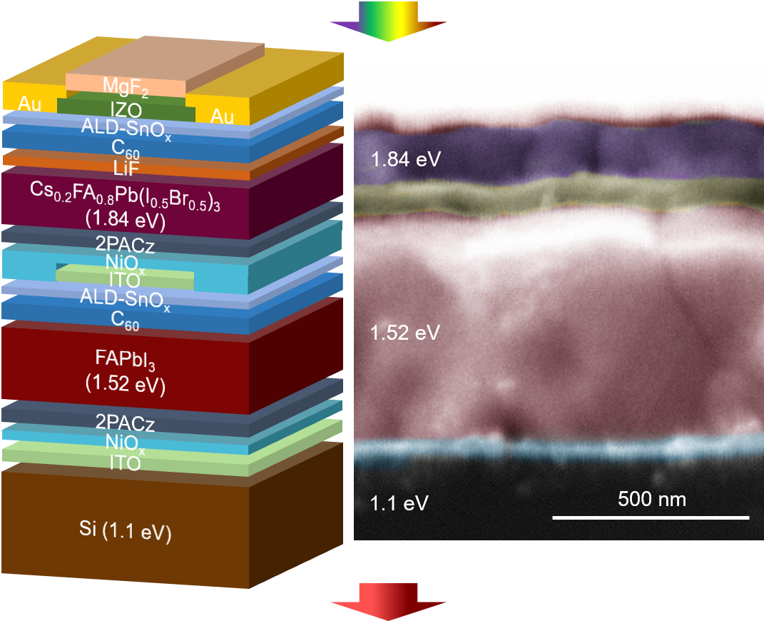
In the study “Triple-junction perovskite–perovskite–silicon solar cells with power conversion efficiency of 24.4%,” published in Energy & Environmental Science, Paetzold and his colleagues explained that the cell was based on a perovskite top cell with an energy bandgap of 1.84 eV, a perovskite middle cell with bandgap of 1.52 eV, and a silicon bottom cell with a bandgap of 1.1 eV.
The bottom cell had a thickness of 200 μm-thick. It was etched with potassium hydroxide, and was based on electron-collecting poly-Si on oxide (POLO) junctions. For the middle and top devices, the scientists used one of the most promising halide perovskites – the α-formamidinium lead iodide known as α-FAPbI3. The recombination junctions were formed by sputtered indium tin oxide (ITO) layers.
“ITO also serves as anchoring oxide for the sequential hole transport layer (HTL), especially for the double HTLs of NiOx/self-assembled monolayer (SAM),” the academics explained. “A double HTL based on a combination of sputtered nickel(II) oxide (NiOx) and carbazole (2PACz) is used in both perovskite subcells, offering an excellent charge carrier extraction, a robust barrier for the solvents of perovskite precursor, and a very good yield for the devices.”
Tested under standard illumination conditions, the triple-junction cell achieved a power conversion efficiency of 24.4%, an open-circuit voltage of 2.84 V, a short-circuit current of 11.6 mA cm–2, and a fill factor of 74%. The research group stated this is the highest efficiency ever reported to date for this kind of triple-junction device.
The cell was also able to retain 96.6% of the initial efficiency in dark storage aging at 85 C for 1,081 h.
“Taking advantage of optical simulations and experimental optimizations in triple junction, the current mismatch was minimized, and current generation was maximized,” Paetzold said. “Key to this achievement was our development of a high-performance middle perovskite sub-cell, employing a stable pure-α-phase high-quality FAPbI3 thin film.”
Paetzold also explained that the middle perovskite sub-cell is beneficial to providing a suitable middle bandgap, very good thermal stability, excellent interfaces to both recombination junctions, and a low density of defects and pinholes.
“Our study opens the door to a new era of perovskite-based high-efficiency triple-junction PV,” he concluded.
This content is protected by copyright and may not be reused. If you want to cooperate with us and would like to reuse some of our content, please contact: editors@pv-magazine.com.


By submitting this form you agree to pv magazine using your data for the purposes of publishing your comment.
Your personal data will only be disclosed or otherwise transmitted to third parties for the purposes of spam filtering or if this is necessary for technical maintenance of the website. Any other transfer to third parties will not take place unless this is justified on the basis of applicable data protection regulations or if pv magazine is legally obliged to do so.
You may revoke this consent at any time with effect for the future, in which case your personal data will be deleted immediately. Otherwise, your data will be deleted if pv magazine has processed your request or the purpose of data storage is fulfilled.
Further information on data privacy can be found in our Data Protection Policy.