From pv magazine Global
An international group of scientists has proposed a new copper indium gallium selenide (CIGS) solar cell structure using antimony trisulfide (Sb2S3) as the back surface field (BSF) layer.
Sb2S3 is a promising candidate for the photovoltaic community owing to the earth-abundant and environmentally friendly constituent elements alongside appropriate optoelectronic properties such as a desirable band gap of around 1.7 eV, large absorption coefficient and long-term stability
BSF layers consist of a higher doped region at the rear surface of the solar cell and are commonly used to increase a device’s voltage. “Sb and S are abundantly available on Earth. Hence, incorporating a thick layer of Sb2S3 in industrial CIGS solar cells can effectively reduce their production costs,” the researchers said. “By reducing the thickness and cost of the CIGS absorber layer, this approach promises to make solar energy more accessible and sustainable.”
They numerically simulated and optimized the solar cell via the SCAPS–1D solar cell capacitance software, developed by the University of Ghent, to simulate the novel cell design.
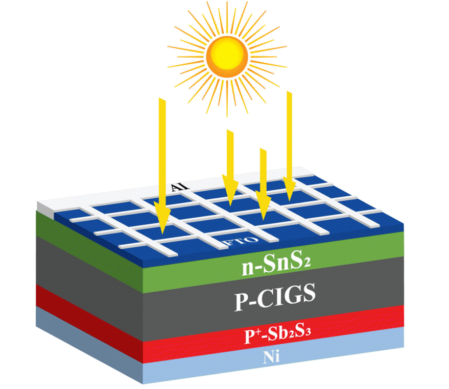
The academics fabricated the cell with a back contact layer made of nickel (Ni), the Sb2S3-based BSF layer, a CIGS absorber, an electron transport layer (ETL) made of tin disulfide (SnS2), a window layer based on fluorine-doped tin oxide (FTO), and a front electrode made with aluminum (Al).
In the simulation, the researchers optimized the thicknesses of the buffer, absorber, and BSF layers. They also investigated acceptor density, defect density, capacitance–voltage (C–V), interface defect density, rates of generation and recombination, operating temperature, current density, and quantum efficiency.
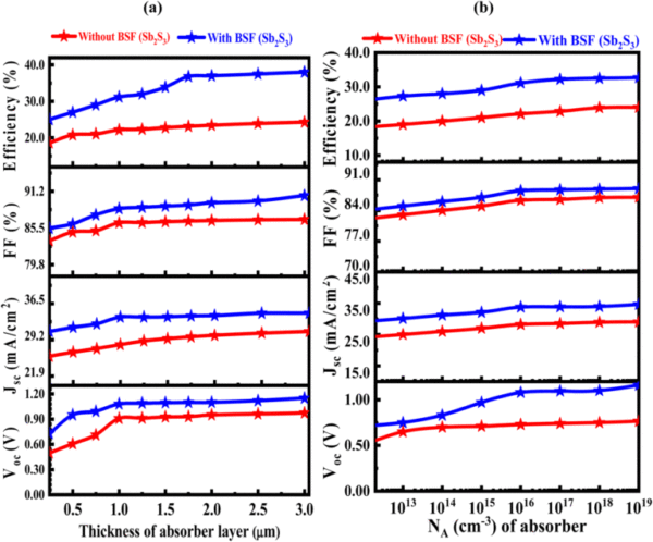
Image: Begum Rokeya University, RSC Advances, CC BY 3.0 DEED
“After details optimization, the optimal thicknesses for the FTO window, CIGS absorber, SnS2 buffer, and Sb2S3 BSF layers are found to be 0.05 μm, 1.0 μm, 0.05 μm and 0.20 μm, respectively,” the group said. “The large thickness of buffer creates the series resistance and absorption losses in the solar cell structure. Since the buffer allows light to enter the solar cell device, so excellent transparency and the right thickness are needed, which is the 0.05 mm for SnS2 buffer in our proposed structure.”
With those optimized parameters, the simulated double heterojunction (DH) cell exhibited a power conversion efficiency of 31.15%, an open-circuit voltage of 1.08 V, a short-circuit current density of 33.75 mA cm2, and a fill factor of 88.50%. A reference CIGS cell optimized and simulated without the Sb2S3 BSF layers achieved an efficiency of 22.14%, an open-circuit voltage of 0.91 V, a short-circuit current density of 28.21 mA cm2, and a fill factor of 86.31%.
“The outcomes of this study provide insights into the development of an ultra-thin Sb2S3 BSF layer, which can be included in conventional CIGS solar cells to improve their efficiency and reduce the absorber material’s cost,” the group concluded.
Its findings and the solar cell concept were presented in the study “Improving the efficiency of a CIGS solar cell to above 31% with Sb2S3 as a new BSF: a numerical simulation approach by SCAPS-1D,” published in RSC Advances. The team included scientists from Bangladesh’s Begum Rokeya University, Hajee Mohammad Danesh Science and Technology University and Pabna University of Science and Technology, as well as from Mexico’s Autonomous University of Querétaro, Iraq’s Al-Karkh University of Science, and Saudi Arabia’s King Khalid University.
This content is protected by copyright and may not be reused. If you want to cooperate with us and would like to reuse some of our content, please contact: editors@pv-magazine.com.


By submitting this form you agree to pv magazine using your data for the purposes of publishing your comment.
Your personal data will only be disclosed or otherwise transmitted to third parties for the purposes of spam filtering or if this is necessary for technical maintenance of the website. Any other transfer to third parties will not take place unless this is justified on the basis of applicable data protection regulations or if pv magazine is legally obliged to do so.
You may revoke this consent at any time with effect for the future, in which case your personal data will be deleted immediately. Otherwise, your data will be deleted if pv magazine has processed your request or the purpose of data storage is fulfilled.
Further information on data privacy can be found in our Data Protection Policy.