Highly selective contacts are the key to achieving high efficiency in thin-film solar cells. These contacts allow one type of carrier (holes) to conduct and block the other type (electrons). Nickel oxide (NiO) is an optimum material for hole-selective contacts and is extensively used in multiple photovoltaic technologies. Nickel oxide films with thicknesses in the nanometre range (a hundred thousand times smaller than the width of a single human hair) must be produced for use in advanced-architecture silicon solar cells.
However, the current process of developing nanometric thin nickel oxide membranes through sputtering is highly expensive as the equipment used in its production has to be imported. Precursor components such as nickel acetylacetonate used in the development of these membranes are also extremely expensive. The cost of this technique limits the possibilities of its use.
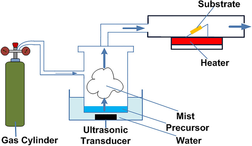
Researchers at the Indian Institute of Technology Mandi (IIT Mandi) have developed a low-cost process to produce ultra-thin films of metal oxides from cheaper starting materials. Specifically, they used an aerosol-assisted chemical vapor deposition technique to deposit nickel oxide thin film on a silicon substrate.
“Aerosol-assisted chemical vapor deposition technique can produce high-quality, uniform thin films on various surfaces, including silicon, by delivering a vapor phase precursor in the form of an aerosol. The aerosol enables the deposition of a wide range of oxide-based materials with high precision, making it a versatile and cost-effective method for various applications in materials science and engineering,” said Kunal Ghosh, who led the study.
The team used nickel nitrate hexahydrate as the nickel salt and the deposition was performed at 550°C for a time period of 15 minutes to produce nickel oxide films with a thickness of approximately 15 nanometres. They analyzed the morphology and composition of the nickel oxide films produced using various characterization techniques. They also analyzed the diode characteristics of the deposited thin film on the silicon substrate and found it to have properties suited for the fabrication of solar cells; the current–voltage measurements showed a diode-like behavior with a current density of 4.54 mA/cm2 obtained at 1 V.
Presently, the project is still in the early stages of development. However, with further development, this technology has the potential to be adopted by the industry. This research will enhance the fabrication process of advanced architecture silicon photovoltaic devices, reducing the cost and complexity of commercial techniques.
Ghosh said, “Our research shows that it is possible to develop a cost-effective and scalable process for the production of metal oxide layers for solar cells. This new method has the potential to revolutionize the solar industry by reducing the cost and complexity of current production techniques. Additionally, as the whole process including the equipment is developed in-house, the generated IP will contribute towards India’s self-reliance in the area of advanced-architecture silicon solar cells.”
This content is protected by copyright and may not be reused. If you want to cooperate with us and would like to reuse some of our content, please contact: editors@pv-magazine.com.


3 comments
By submitting this form you agree to pv magazine using your data for the purposes of publishing your comment.
Your personal data will only be disclosed or otherwise transmitted to third parties for the purposes of spam filtering or if this is necessary for technical maintenance of the website. Any other transfer to third parties will not take place unless this is justified on the basis of applicable data protection regulations or if pv magazine is legally obliged to do so.
You may revoke this consent at any time with effect for the future, in which case your personal data will be deleted immediately. Otherwise, your data will be deleted if pv magazine has processed your request or the purpose of data storage is fulfilled.
Further information on data privacy can be found in our Data Protection Policy.