From pv magazine International
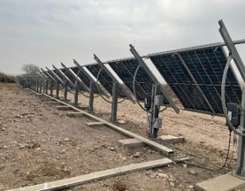
The introduction of larger wafer/cell formats has been one of the biggest recent trends in module technology. With two different sizes – the 210mm ‘G12’ introduced by Zhonghuan Semiconductor, and the smaller 182mm ‘M10’ format produced by Longi – now well established in manufacturing, the industry is looking for ways to differentiate between the two.
Results from various field tests published throughout this year have been able to demonstrate an advantage for either format. New findings published this week by Chinese manufacturer Trina Solar reveal that the 210mm format, used in the company’s Vertex module series, achieved an energy yield as much as 1.6% higher than products based on the 182mm product, over a six month period.
The modules were tested at a site in Yinchuan, China, which has a dry, temperate climate, and a second site in Changzhou, China, where conditions are subtropical with hot, rainy summers and high humidity. At the Yinchuan site, data from April to September 2021 showed a 1.2% energy yield advantage for the Vertex modules, based on monofacial modules installed on fixed-tilt racking at a height of 1 meter. For bifacial modules, the advantage increased slightly to 1.3%. And at the Changzhou site, the Vertex modules reached a yield 1.6% higher than the 182mm products.
Trina Solar’s analysis of the results found that better performance in low-irradiance conditions (200 watts per square meter) was key to the Vertex module’s advantage.
Operating temperature
Higher currents in the larger format products are one of the key differences between the two products, and earlier results presented by JA Solar (which is backing the 182mm format) found that this resulted in a higher operating temperature, and therefore lower energy yield, for the 210mm products. This was not the case in Trina’s field testing, however, with no measurable temperature difference between the two at either site.
Closer analysis of the two test system layouts and components would be needed to understand the reasons for the different operating temperatures (the JA Solar test site is also located in Yinchuan, with similar conditions). For the time being, modules based on both wafer formats will be available on the market. Further field testing, as well as standardization and the development of other system components to suit the characteristics of either format and optimize costs, will show whether either has a real advantage overall or in particular applications.
This content is protected by copyright and may not be reused. If you want to cooperate with us and would like to reuse some of our content, please contact: editors@pv-magazine.com.


By submitting this form you agree to pv magazine using your data for the purposes of publishing your comment.
Your personal data will only be disclosed or otherwise transmitted to third parties for the purposes of spam filtering or if this is necessary for technical maintenance of the website. Any other transfer to third parties will not take place unless this is justified on the basis of applicable data protection regulations or if pv magazine is legally obliged to do so.
You may revoke this consent at any time with effect for the future, in which case your personal data will be deleted immediately. Otherwise, your data will be deleted if pv magazine has processed your request or the purpose of data storage is fulfilled.
Further information on data privacy can be found in our Data Protection Policy.