From pv magazine International
Depositing the various layers that make up a PV cell stack onto a silicon wafer is among the most complex and expensive areas in PV cell & module manufacturing. The processes used here often require the creation of a vacuum, the use of flammable or otherwise hazardous precursor materials, high processing temperatures and other challenges.
A group of scientists led by the Fraunhofer Institute for Solar Energy Systems, in collaboration with the Technical University of Ilmenau in Germany had these factors in mind when it looked at the deposition of silicon dioxide (SiO2), which can be used as a passivation layer or a protective layer in various types of silicon PV cells. The group notes that plasma-enhanced chemical vapor deposition (PECVD) is the most common process used with this material, but requires both high temperatures and a vacuum.
The group looked into alternative processes including spray pyrolysis, low-pressure chemical vapor deposition (LPCVD), sol-gel deposition, and atomic layer deposition, eventually settling on atmospheric pressure deposition (APCVD) as the best option for further investigation. “APCVD holds the advantage of using gases as reactant precursors in contrast to liquids,” the group explains. “Consequently, crack-free dense films with good step coverage can readily be obtained.”
3D printed thermoplastic
Using APCVD, the group was able to demonstrate a low-temperature SiO2 deposition process that also eliminated the use of highly flammable hydrosilane as a precursor material. And since the equipment does not have to withstand very high temperatures, the entire setup could be made of low-cost thermoplastic material produced using 3D printing, making it easily adaptable to different wafer shapes and sizes.
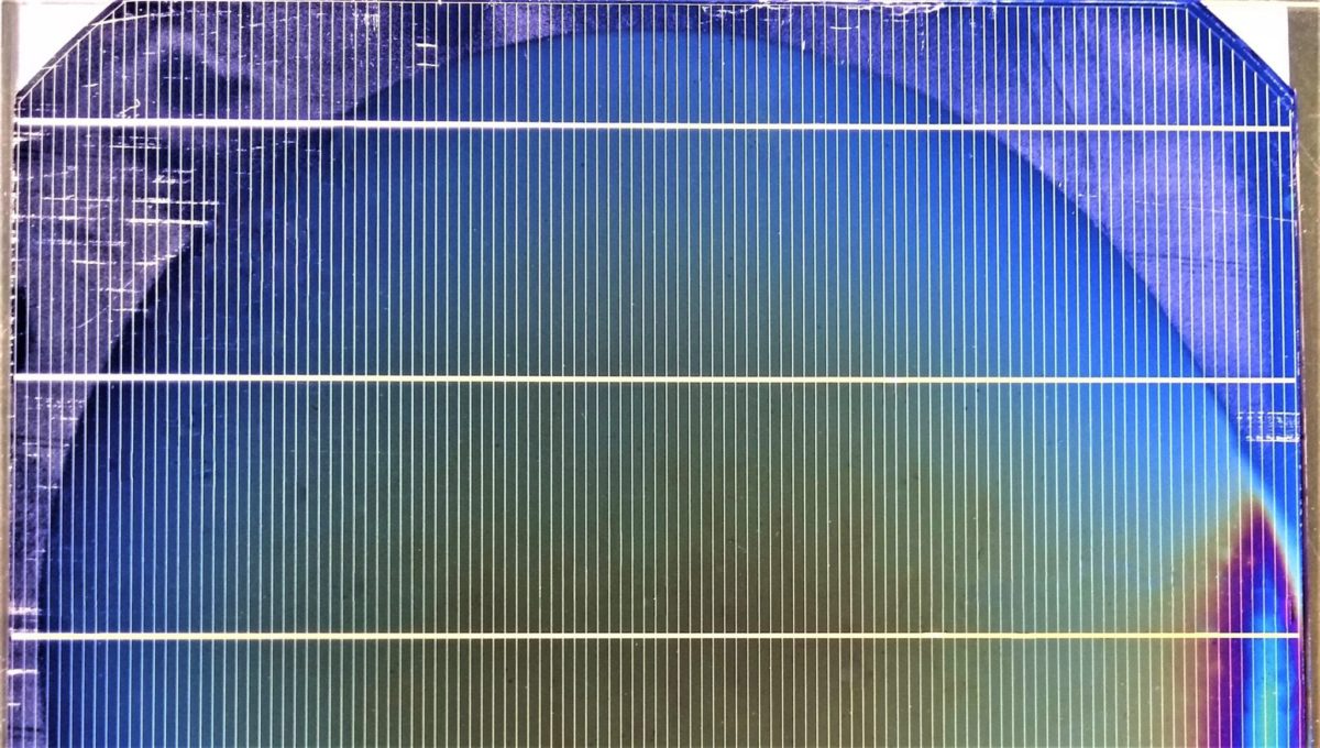
The group investigated two different applications for the setup in solar cell manufacturing. First, single side texturing – wafers were coated on one side with around 180 nanometers of SiO2, and then annealed at 180 degrees Celsius. Secondly, the process used to deposit a protective layer to prevent parasitic plating of metals when laying down the cell fingers and busbars.
In the first application, the wafer was then treated with an alkaline texturing solution, which etched about 100 nm of the SiO2 layer and left a smooth, uniform surface. And in the second application, the SiO2 layer was shown to effectively protect against unwanted metal deposition. “The SiO2 coated areas of the cells were practically free of unwanted metal deposition,” the scientists stated. “Whereas there was massive parasitic plating in the uncoated areas.”
Cell efficiencies were measured between 19.3% and 19.8% – below what has already been achieved in PERC cell production. However, the group notes that its focus was on measuring the performance and reliability of the coating processes, meaning there was less overall focus on the cell efficiency. Full details of the work are found in the paper Application of hydrosilane-free atmospheric pressure chemical vapor deposition of SiOx films in the manufacture of crystalline silicon solar cells, published in Thin Solid Films.
“The newly developed APCVD setup provides a simple and tailorable approach for the deposition of SiO2 films on virtually every substrate material at room temperature,” the group concludes. “Because of the used non-flammable and inexpensive gases, the costs of the deposition equipment and of the operations are low. The presented simple APCVD SiO2 process can find several applications in photovoltaics.”
And work is ongoing to bring the process to an industrial scale, as part of a collaboration with Hannover-based coatings company Alethia, which is currently set to run until May 2022.
This content is protected by copyright and may not be reused. If you want to cooperate with us and would like to reuse some of our content, please contact: editors@pv-magazine.com.


By submitting this form you agree to pv magazine using your data for the purposes of publishing your comment.
Your personal data will only be disclosed or otherwise transmitted to third parties for the purposes of spam filtering or if this is necessary for technical maintenance of the website. Any other transfer to third parties will not take place unless this is justified on the basis of applicable data protection regulations or if pv magazine is legally obliged to do so.
You may revoke this consent at any time with effect for the future, in which case your personal data will be deleted immediately. Otherwise, your data will be deleted if pv magazine has processed your request or the purpose of data storage is fulfilled.
Further information on data privacy can be found in our Data Protection Policy.