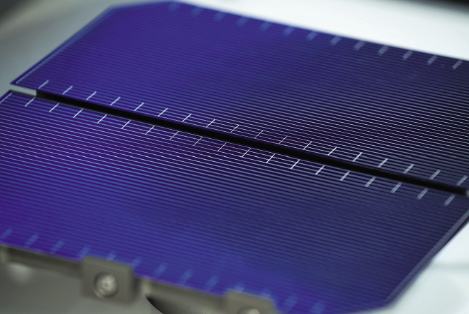
Half cut cell technology has quickly established itself as a reliable and relatively simple method for manufacturers to push more watts out of their modules and meet increasing demand from customers for high-powered products.
In its 2019 bankability survey, BloombergNEF found that 88% of industry participants viewed half cut cell as a bankable technology. “Half cut has good market acceptance, and most manufacturers have mastered the process thanks to mature equipment. Yield has also largely improved and seems no big issue to the product cost,” says Yali Jiang, an analyst on BloombergNEF’s Solar Insight team. “By the end of 2020, half cut is expected to be a standard product.”
Inherent risk
Despite the technology’s maturity and the ability of manufacturers to produce half cells without major damage to the edge, concerns remain over the formation of microcracks during the conventional cutting process, and the effect this could have on long-term module performance. “Anybody that is going to cut their cell, whether for half cut, third cut or shingled modules, you are going to have the risk of microcracks at that edge,” explains Andrew Gabor, CTO at U.S.-based testing equipment supplier BrightSpot Automation. He goes on to explain that these microcracks are typically sub-millimeter in length and do not show up in high-resolution electroluminescence imaging. And since these microcracks do not affect module performance, unless they propagate into larger cracks with discontinued metallization, the modules are still able to pass testing conducted according to present IEC standards. “Later, in the field or during handling, frontside load on the module puts those cells into tensile stress, and the microcracks propagate into full cracks, which are then opened up through thermal cycling or cyclic wind loading.”
As well as cracking, cell-cutting processes risk damage to the cell’s sensitive passivation layers, potentially causing voltage loss. “Passivation on laser ablation cuts is problematic, as half of the surface was molten and is randomly recrystallized,” explains Frederick Bamberg, product manager at laser equipment supplier 3D-Micromac. “This can be overcome using an alternative cutting technology.”
A large number of manufacturers have adopted conventional laser scribing processes for cell cutting, where the rear of the cell is scribed with a laser, and the cell is then broken in two. Though equipment suppliers using this type of process are working on improvements, there is still an inherent risk of microcracking. DR Laser, a PV equipment supplier based in Wuhan, China, told pv magazine that although its process is designed to minimize mechanical stress on cells during splitting, it has noticed the issue of microcracking and damage to passivation layers during cell cutting. It is now working on cost-effective approaches to solving this, although it did not provide additional details.
Fellow Chinese equipment supplier Gsolar says that by narrowing the width of its laser scribe it can reduce the risk of cell damage. “Gsolar uses a special laser process to divide the laser beam into multiple coaxial beams. Compared to a galvanometer cutting process, we retain the advantages of multiple scribing and reduce the groove width by more than 50%,” says Gsolar General Manager Ran Xu. “We can minimize the microcracking by fine grooving without increasing equipment cost. Since the silicon at the crack location is exposed, the damage to the passivation layer is unavoidable. But the damage can be reduced by minimizing the groove size.”
Avoiding cracks
Other equipment suppliers, meanwhile, have sought alternatives to the scribe and break process to eliminate cell damage during cutting. Germany’s 3D-Micromac developed a process it calls thermal laser separation, where cells receive a point defect at a determined position on either side from one laser, are heated along the center line by a second laser, and then rapidly and precisely cooled using a water spray. This causes the cell to separate cleanly in the resulting field of thermal stress. InnoLas Solutions, another Germany-based laser equipment supplier, developed a laser direct cleaving process, in which a laser source handles the cutting of the cell, rather than only scribing. “You induce an initial crack, and you propagate that crack along a determined area,” says InnoLas Solutions CEO Markus Nicht. “And we use the laser to propagate the crack.”
Though their makers are certain that the higher throughput and better performance of these tools results in lower cost of ownership over the long term, the initial investment required is higher and many manufacturers are opting for the conventional processes. “A lot of half-cell sites go for processes like scribe and break,” continues Nicht. “The risk with this is firstly, a lot of particles which can contaminate your cell. Secondly, you generate a lot of microcracks and thirdly you induce so much heat that you sometimes melt over the frontside material and into the bulk material.”
3D-Micromac as well is convinced that, as the half-cell format comes to represent the bulk of modules on the market, differences in quality resulting from the cutting process will become more apparent. “Microcracks introduced when cutting by laser ablation and mechanical cleaving cause significantly higher degradation rates over the life span of modules in operation,” says Frederick Bamberg. “The industry’s focus is on initial efficiency and nominal module power. However, when there is oversupply, and when modules are further evaluated on kilowatt-hours per year, the market will pay more attention to this, and end customers will look for long lasting quality before lowest price.”
This content is protected by copyright and may not be reused. If you want to cooperate with us and would like to reuse some of our content, please contact: editors@pv-magazine.com.


By submitting this form you agree to pv magazine using your data for the purposes of publishing your comment.
Your personal data will only be disclosed or otherwise transmitted to third parties for the purposes of spam filtering or if this is necessary for technical maintenance of the website. Any other transfer to third parties will not take place unless this is justified on the basis of applicable data protection regulations or if pv magazine is legally obliged to do so.
You may revoke this consent at any time with effect for the future, in which case your personal data will be deleted immediately. Otherwise, your data will be deleted if pv magazine has processed your request or the purpose of data storage is fulfilled.
Further information on data privacy can be found in our Data Protection Policy.