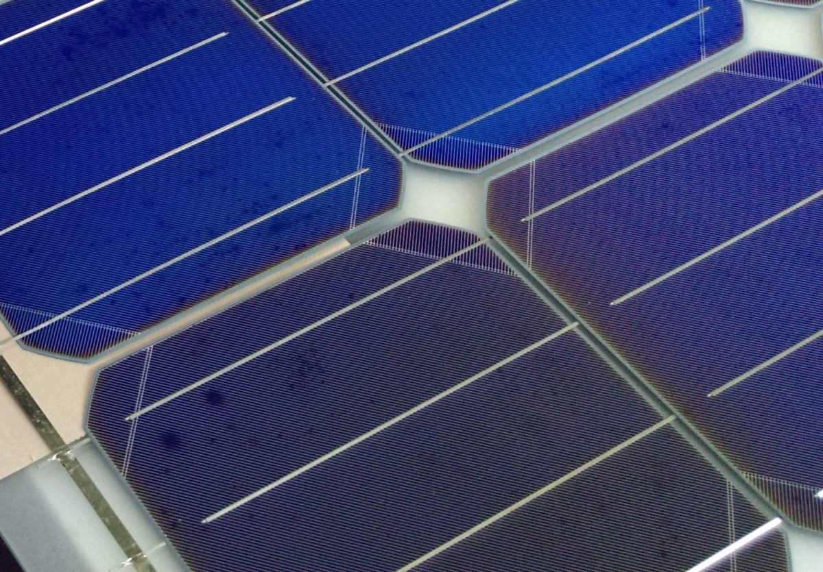
The Institute for Solar Energy Research Hamelin (ISFH) and the Leibniz Universität Hannover claim to have achieved an efficiency of 26.1% for a crystalline silicon solar cell based p-type wafer material at laboratory level. This is a world record for p-type silicon, as well as a European record for crystalline silicon, the two entities said in a statement. The measurement was conducted by ISFH-CalTeC, at its ISO 17025-accredited Calibration and Test Center.
P-type cells currently available on the market achieve an efficiency of between 21% to 22%, although only if combined with PERC cell technology, ISFH told pv magazine. The record efficiency for such cells is 23.4%, while the record for p-type laboratory cells was recently set at around 25%.
“Our cell is now significantly above 26.1%,” said project manager Felix Haase. For comparison, the average efficiency of n-type wafers is 26.7%, he added. Efficiencies above 25% have been achieved with n-type silicon only in combination with boron or heterojunctions of amorphous silicon.
“Our results show that neither n-type silicon nor boron or amorphous silicon is a must for ultra-high efficiencies. There are other attractive ways to achieve the highest levels of silicon efficiency at potentially low cost,” explained Rolf Brendel, Managing Director of ISFH.
The record cell uses a passivating electron-selective n+-type polysilicon on oxide (POLO) junction at the minus contact of the cell and a hole-selective p+-type POLO junction at the plus contact., the research institute stated. The high selectivity of these junctions would be responsible for the higher efficiency, as they are applied in an interdigitated pattern on the rear side, thus minimizing the parasitic absorption in the poly-Si, and avoiding shading by front side metallization.
The ISFH plans to replace the process steps with industry-related process steps in the coming years. The goal is the integration of the POLO junctions into the current mainstream technology. “Replacing photolithography by laser contact opening is a first important step towards industrialization as it enables screen-printing-based metallization,” said the research group coordinator Robby Peibst.
Germany’s Federal Ministry of Economy and the State of Lower Saxony have financially backed the research.
Author: Daniel Seeger
This content is protected by copyright and may not be reused. If you want to cooperate with us and would like to reuse some of our content, please contact: editors@pv-magazine.com.


By submitting this form you agree to pv magazine using your data for the purposes of publishing your comment.
Your personal data will only be disclosed or otherwise transmitted to third parties for the purposes of spam filtering or if this is necessary for technical maintenance of the website. Any other transfer to third parties will not take place unless this is justified on the basis of applicable data protection regulations or if pv magazine is legally obliged to do so.
You may revoke this consent at any time with effect for the future, in which case your personal data will be deleted immediately. Otherwise, your data will be deleted if pv magazine has processed your request or the purpose of data storage is fulfilled.
Further information on data privacy can be found in our Data Protection Policy.