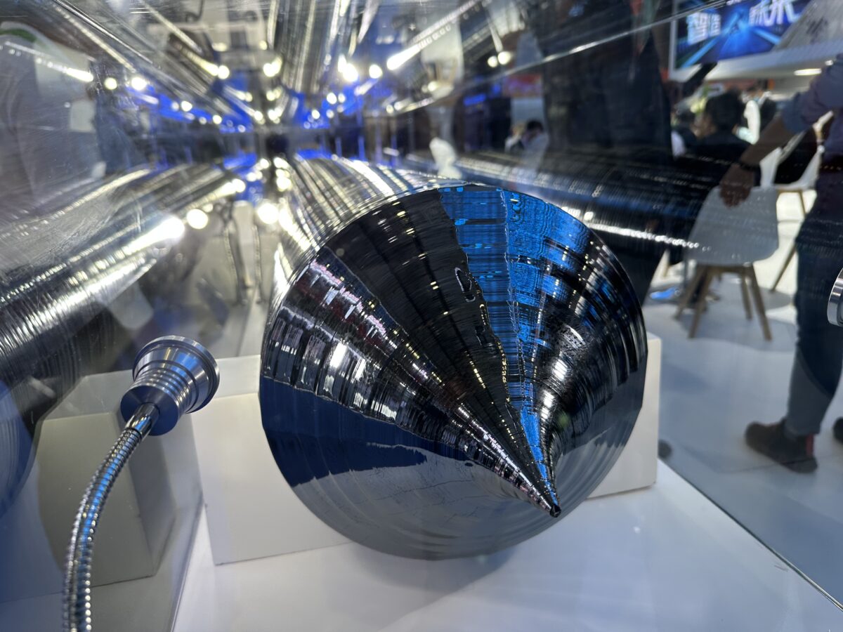
A team led by the Australian National University has investigated antimony (Sb)-doped Czochralski-grown silicon as an alternative n-type substrate for solar PV applications in a study that included the characterization of axial resistivity distribution, donor properties, and mechanical strength.
“This study elucidated why antimony-doped n-type silicon ingots can achieve uniform resistivity distribution despite antimony’s very low segregation coefficient. We demonstrated that the key factor is the controlled evaporation rate of Sb during Czochralski growth, not co-doping with phosphorus as often speculated,” corresponding author, Rabin Basnet, told pv magazine.
The research, which appears in “Resistivity distribution and donor properties of antimony-doped n-type Czochralski silicon ingots,” published in Solar Energy Materials and Solar Cells, helps to “explain how industry has managed to produce uniform Sb-doped ingots and provides a scientific basis for optimizing doping uniformity in next-generation wafers,” according to Basnet.
Although the use of Sb for wafer doping in photovoltaic applications is novel, Sb is a “well-established n-type dopant” in semiconductor device manufacturing, according to the researchers.
In previous work on the topic, “High Quality Antimony-Doped n-Type Silicon Wafers for Solar Cell Applications,” published in Solar RLL, the group showed that “switching the donor dopant from phosphorus to antimony does not compromise the bulk lifetime” of n-type Czochralski (Cz) wafers, according to Basent.
“Building on that, the present paper shows that antimony doping also enables highly uniform resistivity along the Cz-Si ingot’s axial direction. Together, these findings indicate that Sb-doped n-type Cz wafers are considered a strong candidate to become the industry standard for the next generation of n-type wafers,” said Basent.
The researchers used Sb- and phosphorous-doped (P-doped) silicon wafers that were grown via the recharged Cz ingot growth process and supplied by Chinese manufacturer Longi Green Energy Technology. For testing, it relied on electron paramagnetic resonance (EPR) spectroscopy to assess donor and dopant-related characteristics and electrical resistivity. Standard testing of the bending strength was done with a three-point bending setup.
As for modelling, the team noted that to evaluate the viability of Sb for this application, the conventional model based on Scheil’s equation had to be modified to account for both “segregation and evaporation effects as the mechanisms of incorporation.”
“It was initially surprising that Longi achieved such a uniform resistivity distribution using only Sb doping. Given that antimony has a segregation coefficient almost an order of magnitude lower than phosphorus, one would expect significant axial variation. Our analysis, however, revealed that precise control of Sb evaporation during crystal growth, rather than co-doping (as revealed by EPR analysis), explains the observed uniformity, an unexpected and technically elegant solution,” explained Basnet.
The significance of the findings for manufacturers is that uniform resistivity distribution increases usable ingot yield, improving wafer production efficiency, and lowering material costs, according to Basnet, who added that a benefit of the mechanical strength of Sb-doped wafers is reduced breakage during cell processing, enhancing throughput and yield.
The research team intends to continue to investigate Sb doping, including its impact on carrier lifetime, defect formation, and minority-carrier recombination behavior. Plans include comparative studies of thermal stability between Sb-doped and P-doped wafers during processing, along with device-level evaluation of Sb-doped wafers in high-efficiency solar cells to assess electrical and reliability performance, according to Basnet.
The research team included participants from Longi Green Energy Technology, Colorado School of Mines, and the U.S. Department of Energy’s National Renewable Energy Laboratory.
Last year, a research team from ANU and Longi reported the results of an investigation of gettering for n-type wafer quality improvements, as reported by pv magazine.
This content is protected by copyright and may not be reused. If you want to cooperate with us and would like to reuse some of our content, please contact: editors@pv-magazine.com.


By submitting this form you agree to pv magazine using your data for the purposes of publishing your comment.
Your personal data will only be disclosed or otherwise transmitted to third parties for the purposes of spam filtering or if this is necessary for technical maintenance of the website. Any other transfer to third parties will not take place unless this is justified on the basis of applicable data protection regulations or if pv magazine is legally obliged to do so.
You may revoke this consent at any time with effect for the future, in which case your personal data will be deleted immediately. Otherwise, your data will be deleted if pv magazine has processed your request or the purpose of data storage is fulfilled.
Further information on data privacy can be found in our Data Protection Policy.