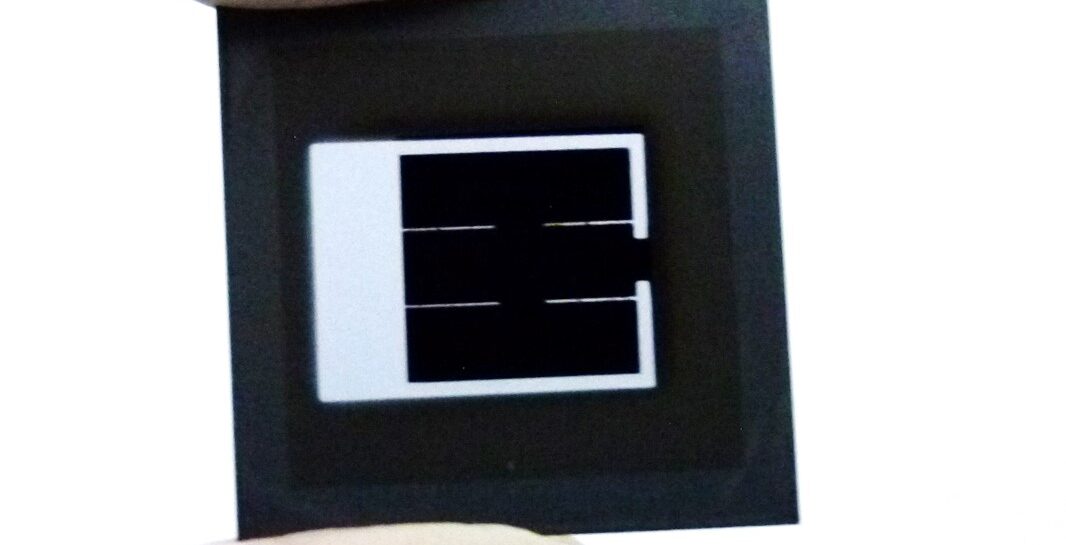
Scientists in China, led by a research team from the PV Technology Center of Tongwei Co., Ltd, a unit of Chinese vertically integrated solar manufacturer Tongwei, used a lower temperature, sequential annealing process to fabricate two-terminal, tandem solar cells that had a wide-bandgap (1.73 eV) perovskite top cell on a fully-textured commercial crystalline silicon heterojunction (SHJ) bottom cell.
“With a carefully modulated sequential annealing process in ambient, we obtain high-quality wide-bandgap perovskite films conformally grown on fully textured silicon substrates with reduced defects and homogeneous composition distribution, enabling the achievement of perovskite-silicon tandems with a certified power conversion efficiency (PCE) of 31.4%, which is among the best-performing tandem devices utilizing commercial silicon sub-cells,” Yuchao Hu, corresponding author of the research, told pv magazine.
The champion tandem device was certified by the National Institute of Measurement and Testing Technology (NIMTT) and by the Fujian Institute of Metrology (FJIM).
The research is described in “Crystallization Modulation of Wide-Bandgap Perovskites on Textured Silicon for Tandem Solar Cells,” published in ACS Energy Letters.
Aware of the challenges of using a conventional evaporation-solution two-step method to form wide-bandgap perovskites on commercial SHJ silicon bottom cells, the research team investigated ways to overcome moisture and thermal-induced complex effects on the crystallization and degradation of perovskite films.
The team investigated the perovskite phase transition process to reveal the crystallization kinetics mechanism of wide-bandgap perovskites, “clarifying the influence mechanisms of external conditions,” such as humidity and heat on film crystallization.
“To overcome the complex issue, we developed a sequential crystallization strategy and realized fine modulations on both the organic halide diffusion and perovskite recrystallization processes. This innovative strategy enabled the fabrication of conformally grown high-quality wide-bandgap perovskite films featuring chemically homogeneous components and reduced defects on silicon cells with large pyramids,” specified Hu.
It is a strategy that has industrial transfer potential. “The annealing process requires temperatures as low as 100-150 C and durations under half an hour,” said Hu, explaining that such conditions are “readily achievable” with established industrial annealing equipment, such as tunnel furnaces, “demonstrating strong potential for process scale-up.”
The perovskite material for the top cell was made of formamidinium iodide (FAI), formamidinium bromide (FABr), cesium bromide (CsBr), plus additives.
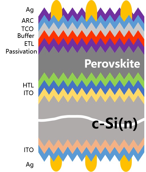
The SHJ subcells were based on n-type, fully textured silicon wafers with a thickness of 110 μm. A transparent conductive oxide (TCO) coating was deposited on the rear side, followed by silver (Ag) electrodes, and on the front side an indium tin oxide (ITO) layer was deposited.
The stack of the p-i-n structured perovskite subcell was as follows: nickel-oxide (NiOx) hole-transport layer (HTL), 2PACz, lead iodide (PbI2) framework layer, perovskite absorber, ethylenediammonium diiodide (EDAI2) passivation, buckminsterfullerene (C60) electron transport layer, SnOx buffer layer, TCO, Ag contacts, lithium fluoride (LiF) anti-reflection coating (ARC).
The energy bandgap of the perovskite films is 1.73 eV, which “well meets the light management demand for the employed 110 μm commercial c-silicon wafers,” noted the researchers.
One of the best-performing target devices was certified with an efficiency of 31.4%, an open circuit voltage of 1.905 V, a fill factor of 81.20%, and a short-circuit current density of 20.30 mA/cm2. It outperformed the control device prepared using the conventional annealing procedure, which had an efficiency of 29.43%, an open-circuit voltage of 1.915 V, a fill factor of 75.67%, and a short-circuit current density of 20.31 mA/cm2.
Collaborating on the research was a team from the University of Electronic Science and Technology of China.
The team is now directing its attention to “the large-area manufacturing of full-size 210 tandem solar cells, industry-standard tandem modules, and their operational stability under outdoor working conditions,” according to Hu.
In a statement about the research, Tongwei said that its perovskite-silicon tandem cell research laboratory was established in the third quarter of 2022 to industrialize tandem cells following a technology roadmap that is compatible with its existing heterojunction production lines. “The focus is on overcoming key mass production technical bottlenecks in tandem cell design, textured surface conformal film formation, interface passivation, low-temperature metallization, and module encapsulation,” it said. The company also said that it plans a megawatt-scale tandem pilot line to be built this year.
This content is protected by copyright and may not be reused. If you want to cooperate with us and would like to reuse some of our content, please contact: editors@pv-magazine.com.


By submitting this form you agree to pv magazine using your data for the purposes of publishing your comment.
Your personal data will only be disclosed or otherwise transmitted to third parties for the purposes of spam filtering or if this is necessary for technical maintenance of the website. Any other transfer to third parties will not take place unless this is justified on the basis of applicable data protection regulations or if pv magazine is legally obliged to do so.
You may revoke this consent at any time with effect for the future, in which case your personal data will be deleted immediately. Otherwise, your data will be deleted if pv magazine has processed your request or the purpose of data storage is fulfilled.
Further information on data privacy can be found in our Data Protection Policy.