From pv magazine International
German engineering association, Verbandes Deutscher Maschinen- und Anlagenbau (VDMA) yesterday published an update to its 2021 International Technology Roadmap for Photovoltaics (ITRPV) report first published in April.
The annual report provides an outlook on which technologies and materials will be implemented in PV manufacturing in the coming years, based on information voluntarily provided by manufacturers. This week’s update features additional discussion of the readiness level for various solar manufacturing technologies, and a ranking that clarifies which of the report’s forecasts rely on expected improvements to current manufacturing process, or the implementation of new techniques not yet available in mass production.
Large wafer formats
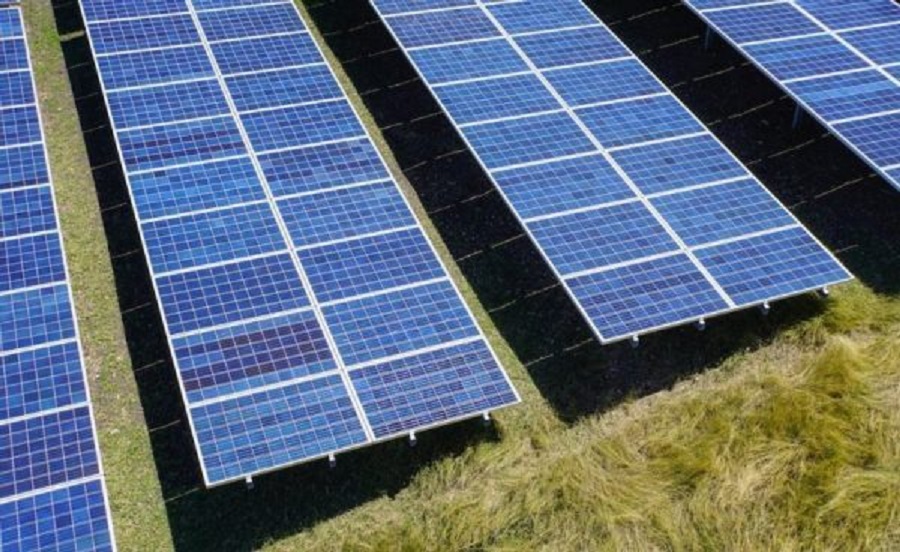
The introduction of new sizes for silicon wafers, primarily 182mm and 210mm, has been the biggest story in PV manufacturing for the past couple of years already, and processes all along the supply chain have had to be adapted to suit these new sizes.
The key takeaway in this ITRPV update is that the largest size, 210mm, still requires development of processes not yet used in mass production to keep up with the production cost of smaller formats, including 182mm. And most analysts predict an initial advantage for 182mm, with 210mm taking a larger share by the second half of the 2020s.
The challenge, according to VDMA, comes in matching the throughput – the number of cells that can be processed per hour. “An evaluation of the technology maturity level of the throughput in cell production shows that the readiness level of the throughputs across all process steps is analogous for the sizes 166 (+/-0.25) mm² and 182 (+/-0.25) mm²,” stated the association. “In contrast, the readiness level related to the throughputs of cell production of the larger wafer format of 210 (+/-0.25) mm² shows that more development work is required in the future.”
Looking at PERC technology, VDMA’s survey finds that the metallization and chemical processing stages of cell production already have mature solutions to process 210mm cells, and for these all sizes are expected to develop in unison – with metallization set to reach 12,000 cells per hour by 2028.
Thermal processing stages, meanwhile, are somewhat slower to run. And here VDMA notes that for 210mm cells to match the expected 11,000 cells per hour throughput that’s expected for smaller formats, more work will be needed. “An evaluation of the technology maturity level of the throughput in cell production shows that the readiness level of the throughputs across all process steps is analogous for the sizes 166 (+/-0.25) mm² and 182 (+/-0.25) mm,” reads the report. “In contrast, the readiness level related to the throughputs of cell production of the larger wafer format of 210 (+/-0.25) mm shows that more development work is required in the future.”
This content is protected by copyright and may not be reused. If you want to cooperate with us and would like to reuse some of our content, please contact: editors@pv-magazine.com.


6 comments
By submitting this form you agree to pv magazine using your data for the purposes of publishing your comment.
Your personal data will only be disclosed or otherwise transmitted to third parties for the purposes of spam filtering or if this is necessary for technical maintenance of the website. Any other transfer to third parties will not take place unless this is justified on the basis of applicable data protection regulations or if pv magazine is legally obliged to do so.
You may revoke this consent at any time with effect for the future, in which case your personal data will be deleted immediately. Otherwise, your data will be deleted if pv magazine has processed your request or the purpose of data storage is fulfilled.
Further information on data privacy can be found in our Data Protection Policy.