From pv magazine 10/2020
PVEL’s Product Qualification Program puts modules through three stages of mechanical stress testing, with thermal cycling and humidity freeze tests designed to open up cracks and reveal the susceptibility of modules to cracking after deployment.
At less than 200 microns thick, silicon solar cells are fragile by nature. At various stages in production, transport, installation, and even after deployment, tiny cracks can appear in a cell. And at the module and system level, this can spell bad news. “Microcracks will eventually grow or branch out, electrically disconnecting large areas of the affected cells,” explains George Touloupas, director of technology and quality at CEA. “Losses will be even higher at string level due to mismatch. Depending on the extent of the cracking, severe hotspots may also occur, risking glass breakage and polymer burnout. If the bypass diodes are triggered, power degradation will be even bigger, as full module substrings will be disconnected.”
There are multiple ways that cracking can start. First, soldering processes: As you cool down from the soldering temperature, copper in the wire contracts more than the silicon, effectively pulling it apart and causing cracks at the surface. Second is cell cutting – while a half-cut cell is mechanically stronger and less susceptible to cracking than a full cell, certain cutting processes are known to leave damage and microcracks along the cut edge (see box p.64). Cracking can also be caused by frontside impacts such as hail, rough handling, and other instances in the field, particularly in harsh weather conditions. “
If modules get below -30 degrees, then there is some bending of the wafer around the interconnect wires where the EVA is thicker to the right and left of the wire than it is above the wire,” explains Andrew Gabor, CTO at Brightspot Automation. “As it cools down, it contracts more to the right and left and kind of bends the wafer around the wire. That can be enough stress to create microcracks.”
Once a cell has microcracks, it is mechanical stress that causes these to propagate. This can come from rough handling in transport or installation, as well as snow or wind. Testing carried out by Brightspot Automation has shown that even a single mild storm can be enough to cause cracks to propagate. “In a standard glass-backsheet module, the cells are not in the neutral axis mechanically,” says Gabor. “You have a thick, stiff piece of glass in front, and a thin, flexible plastic behind. If you press on the frontside of the module, it puts the cells under tensile stress, where they are being pulled apart.”
Mitigation by design
Cracking can progress slowly, affecting module performance over years in the field. Studies show that a crack won’t begin to noticeably affect performance until it has already rendered 8% of a cell’s surface inactive. All of this means problems may not be spotted until long after the point they could be easily fixed, and determining cause and assigning responsibility can be a particularly complex and expensive process.
One way to mitigate cell cracking, and to better understand different modules’ long-term susceptibility to it, is through testing that puts modules through the type of mechanical stress they might see in the field. And here, according to some, is where current standards fall short. IEC 61215, the standard testing requirement for silicon PV modules published by the International Electrotechnical Commission, includes a static mechanical loading test – where bricks or sandbags are stacked on top of the module, up to 2,400 or 5,400 pascals. There is also a hail test, and modules must pass these without physical damage and no more than 5% performance loss. “The issue here is that there is no thermal cycling or anything after the stress test to really try to open up those cracks and show the performance loss,” says Tristan Erion-Lorico, head of PV module business at PV Evolution Labs (PVEL). “There is also no requirement for EL [electroluminescence] imaging. So the module could be utterly destroyed, but because the cracks weren’t fully opened across the metallization, the power is still acceptable, and it passes.”
In its Module Product Qualification Program test sequences, PVEL has incorporated further stages of mechanical stress testing, designed to test susceptibility to cracking to the limit of what could be experienced in the field. After the initial mechanical load test, modules are subjected to a dynamic mechanical load, followed by 50 thermal cycles from 85°C down to -40°C, and then a 10-cycle humidity freeze, where the module is saturated in moisture – 85% humidity at 85°C, and then rapidly cooled again to -40°C.
And PVEL’s initial results paint a mixed picture. The EL images taken after testing (see photos on p.63) show plenty of inactive cell areas due to cracking. However, many of the technologies that have recently gained ground in mass production appear to have the added benefit of reducing crack susceptibility. First off, multi busbar technology was shown to be more resistant to cracking related losses than five-busbar configurations, because even with quite significant cracking, the additional busbars reduce the chance of any cell area being isolated with electrons unable to flow out. Despite the potential risks borne by the cutting process, modules made up of half-cut cells also performed well in stress testing, likely because this layout spreads the pressure between more cells, meaning that each individual cell has to endure less stress.
It is still early days in this testing, however, and there are many more factors that could potentially affect crack susceptibility. “As the industry moves to mono/half cut/multi busbar, crack susceptibility should be improving,” explains Erion-Lorico. “These results are encouraging, but I think it will be a couple of years before we are able to make ‘broad strokes’ statements. Individual bills of material still need to be tested.”
Indeed, there are many more factors to consider in solar PV module design that may contribute significantly to crack susceptibility, and testing for all of these should keep laboratories busy for now. “This area deserves more attention,” explains Gabor. “Factors such as encapsulant thickness and modulus, metal paste composition and microstructure, plated metal vs. paste metal, finger dimensions, and module deflection vs. load are all likely to be important.”
Newer developments in manufacturing as well – high-density modules, larger wafers, and more – will further change the picture with regard to cracking. So, while it may be technically possible to design crack susceptibility out of PV modules entirely, it’s unlikely that we’ll see this happen in the next few years.
Factory floor
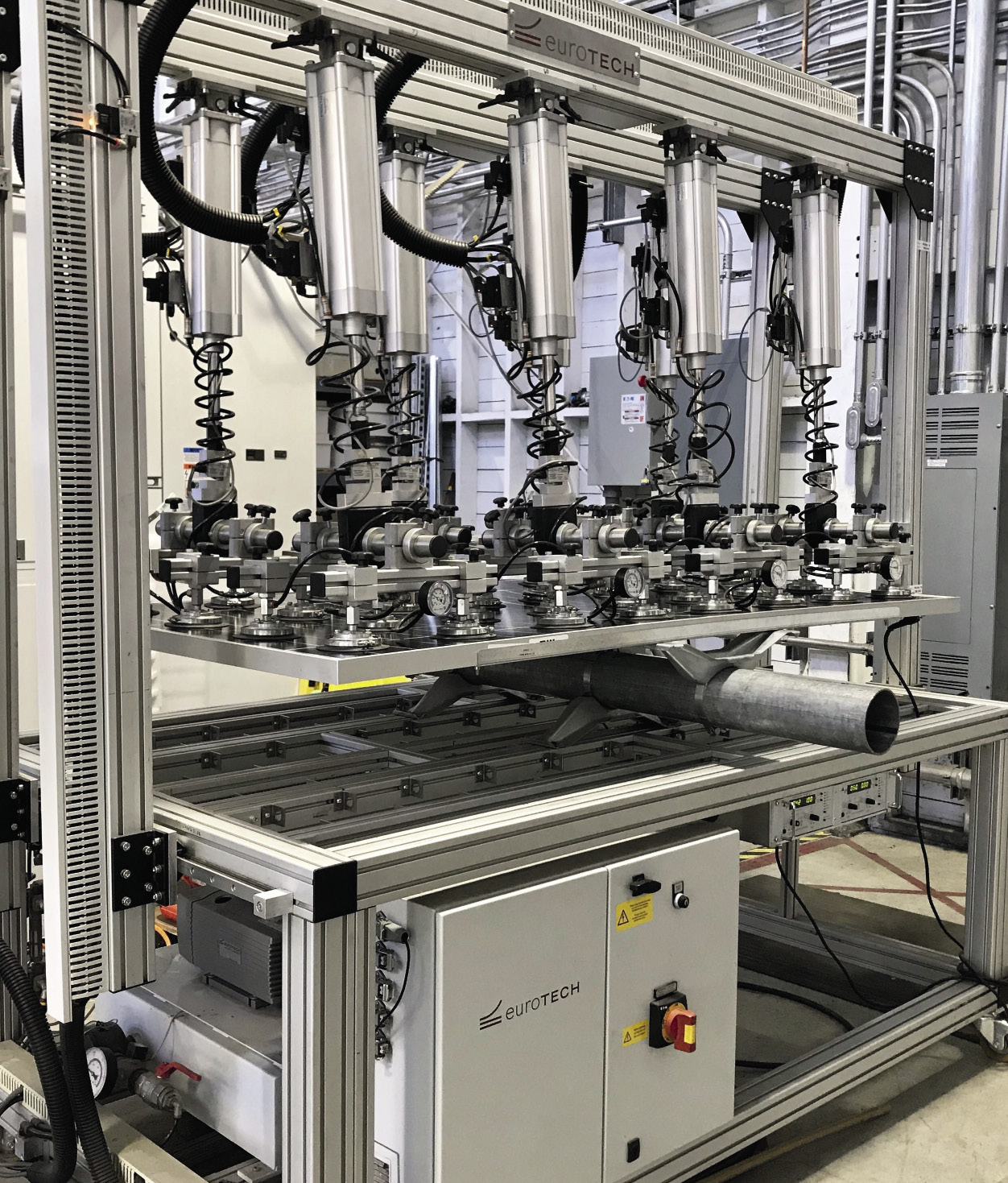
Keeping a close eye on manufacturing processes is one effective way to keep cracking to a minimum. “Silicon is fragile, and automation in PV has to be low-cost for the module prices to be competitive, so cracking cannot be entirely eliminated,” says CEA’s Touloupas. “However, there are many things that can be done to ensure that the effect is not detrimental beyond an acceptable level.” He adds that the automation of interconnection at the layout station and the addition of EL inspection at the tabber-stringer stage, where rework and repairs can still be made with relative ease, are positive developments. However, he also notes that the rate of repairs is a vital metric for quality auditors to monitor and that if it goes too high, additional manual handling may actually lead to more cracking.
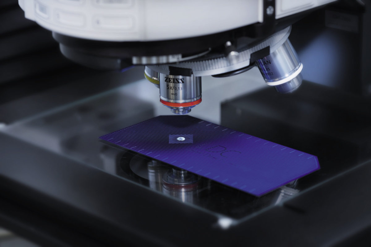
In the production environment, EL testing is key to spotting cracks and preventing modules with cracked cells being shipped. And there may be more that can be done here.
“Many factory EL images I have seen suffer from problems such as low pixel count, poor contrast, poor focus, and poor choice of camera settings,” says Gabor. “With little extra effort and cost, these images could be much improved, allowing for better quality control and feedback to the factory lines.” Touloupas also notes that when conducting factory audits, ensuring that both EL camera settings and operator inspection criteria are effective in detecting cracks should be on engineers’ checklists.
As for the standards, many in the industry see the benefit of adding more testing for crack susceptibility, and an upcoming update to IEC 61215 is expected to specify ‘crack opening’ steps after the initial mechanical load, similar to the additional thermal cycling and humidity freeze tests specified by PVEL. And this could be what’s needed to bring this historically underestimated issue to the front of the industry’s mind. “We have seen clearly on our LoadSpot tool how closed cracks open up with cyclic loading,” says Gabor. “I imagine that a lot of module designs will struggle as we implement crack opening tests following crack creation steps.”
Cell cutting without the cracks
This content is protected by copyright and may not be reused. If you want to cooperate with us and would like to reuse some of our content, please contact: editors@pv-magazine.com.


Good coverage on topic