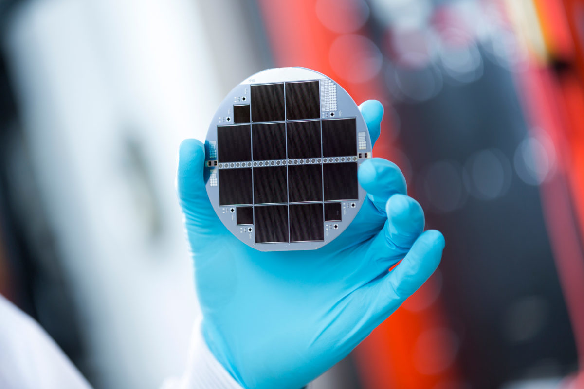
Germany’s Fraunhofer Institute for Solar Energy Systems ISE and equipment manufacturer, EVG have achieved a new efficiency record of 33.3% for a silicon-based multiple solar cell.
The researchers achieved the high conversion efficiency with 0.002 millimeter thin semiconductor layers – less than a twentieth of the thickness of a hair – from III-V compound semiconductors, which were deposited onto a silicon solar cell.
“The layer of the comparatively expensive III-V semiconductor material is so thin that ultimately the material costs are no obstacle,” Frank Dimroth from Fraunhofer ISE told pv magazine. With the success that has now been achieved, Fraunhofer aims to demonstrate the potential of the technology, which achieves a significantly higher degree of efficiency compared to conventional silicon cells.
As early as November 2016, the German solar researchers had demonstrated an efficiency of 30.2% with their industrial partner EVG, a result which was then improved to 31.3% in March 2017. Now they have been able to significantly improve the absorption of light and the charge separation in the silicon, thus achieving the new record value, they said.
The researchers combined the 1.9 micron thin III-V semiconductor layers with the silicon using a process known from microelectronics, direct wafer bonding. The surfaces were deoxidized in a high-vacuum chamber using an ion beam and then pressed together under pressure. The atoms of the III-V surface then formed bonds with the silicon.
The solar cell, which does not have the same complex internal structure of conventional silicon solar cells, has a simple front and back contact and, like conventional cells, can be integrated into solar modules.
“So-called ‘tunnel diodes’ internally connect the three subcells made of gallium-indium-phosphide (GaInP), gallium-arsenide (GaAs) and silicon (Si), which span the absorption range of the sun’s spectrum. The GaInP top cell absorbs radiation between 300 and 670 nm. The middle GaAs subcell absorbs radiation between 500 and 890 nm and the bottom Si subcell between 650 and 1180 nm, respectively,” the scientists explained.
The next step would be to develop the equipment for future large-scale production, said Dimroth. “So far, we need four hours to coat the four square centimeter area – for competitive manufacturing, we need to be able to coat much larger areas within minutes.”
He estimates that another five to 10 years will pass before mass production is possible. Nevertheless, Dimroth expects great cost reduction potential. “Even in the production of conventional silicon solar cells, the cost of large-scale production has been reduced by a factor of 100,” he said.
On the way to industrial production, in particular, the costs of III-V epitaxy and the bonding technology with silicon would have to be further reduced.
The results and efficiency record have now been published in the journal “Nature Energy”.
Author: Daniel Seeger
This content is protected by copyright and may not be reused. If you want to cooperate with us and would like to reuse some of our content, please contact: editors@pv-magazine.com.


By submitting this form you agree to pv magazine using your data for the purposes of publishing your comment.
Your personal data will only be disclosed or otherwise transmitted to third parties for the purposes of spam filtering or if this is necessary for technical maintenance of the website. Any other transfer to third parties will not take place unless this is justified on the basis of applicable data protection regulations or if pv magazine is legally obliged to do so.
You may revoke this consent at any time with effect for the future, in which case your personal data will be deleted immediately. Otherwise, your data will be deleted if pv magazine has processed your request or the purpose of data storage is fulfilled.
Further information on data privacy can be found in our Data Protection Policy.