The PV industry has so far substantially failed to use high-resistivity, lightly doped wafers in commercial solar cell production, although they have fewer recombination sites, improving electrical performance. These wafers, in fact, are more brittle and prone to cracking during handling, sawing, or module assembly.
In contrast, standard Czochralski-grown silicon silicon wafers with moderate to low resistivity are more robust mechanically and easier to process. Moreover, they tolerate thermal and mechanical stress better, which is why they dominate mass-market PV production, despite slightly lower efficiency potential.
In an effort to reduce this gap, Chinese manufacturer Longi and researchers from China’s Sun Yat-sen University have proposed to use edge passivation as a way to increase the mechanical resistance of high-resistivity wafers while maintaining high efficiency and fill factor levels.
“Having potential is not enough,” the research’s lead author, Hao Lin, told pv magazine. “In our early experiments, high-resistivity wafers often performed worse than standard wafers. Our study reveals why. We found that high-resistivity wafers operate at higher excess carrier densities at the maximum power point (MPP) and exhibit reduced carrier collection ability due to flatter concentration gradients. This intrinsic characteristic renders them far more sensitive to edge recombination. Without effective passivation, the edges act as a ‘drain’ that negates the theoretical benefits.”
“We demonstrated that only by coupling high-resistivity wafers with our in-situ edge passivation can this sensitivity be managed, unlocking their true performance,” he went on to say. “Our key insight is that high-resistivity wafers enter this high-level injection regime much more readily than low-resistivity ones. This specific physical characteristic is what grants high-resistivity wafers their superior intrinsic potential for high fill factors.”
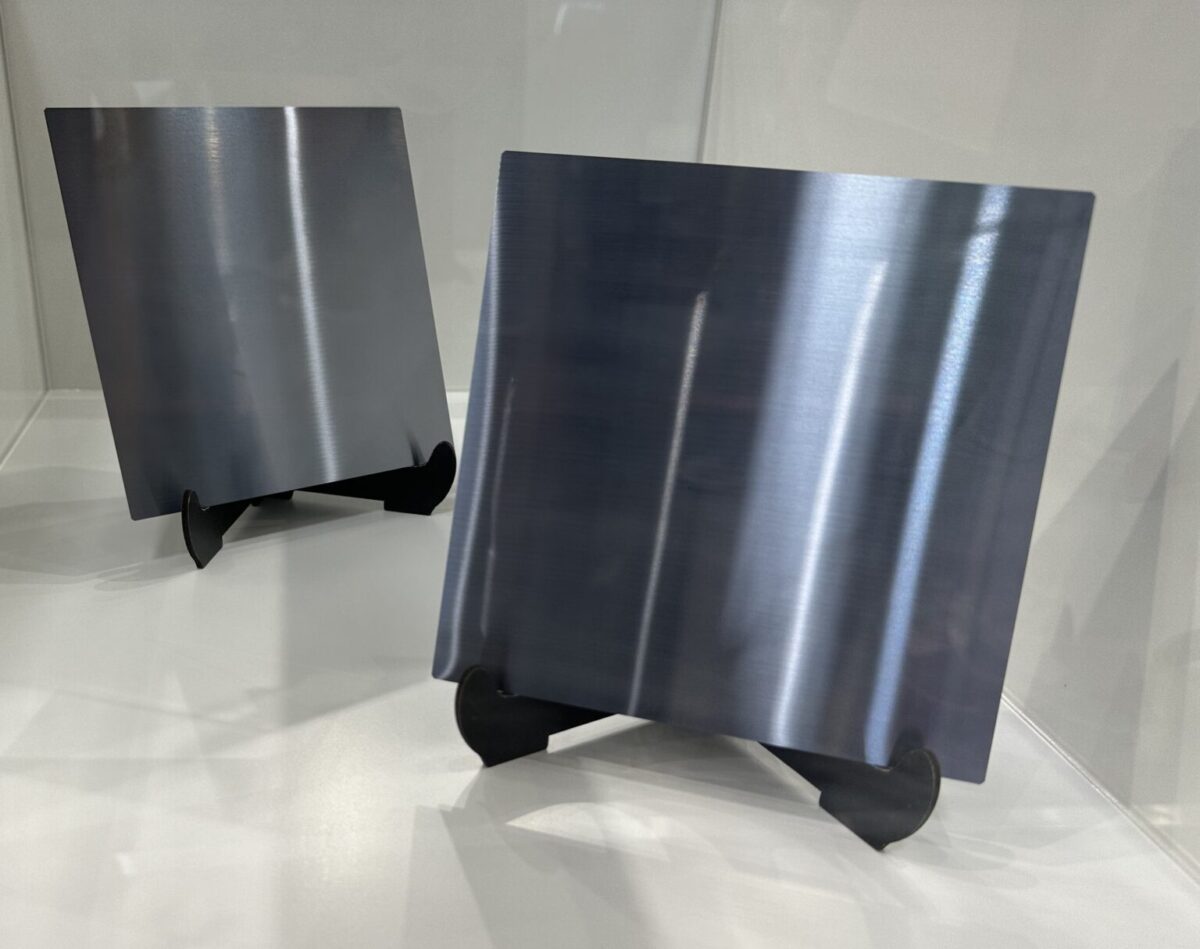
The research team built 182 mm x 91 mm hybrid interdigitated back-contact (HIBC) solar cells using either high-resistivity or Czochralski-grown wafers. They explained that the only difference in the manufacturing process was that silicon nitride was not deposited on the wafer edges of the high-resistivity substrates during chemical vapor deposition. As a result, the unprotected silicon oxide and polysilicon (SiOx/n-poly-Si) passivation layer at the edges was removed during wet chemical cleaning.
The whole manufacturing process consisted of wet chemical cleaning, chemical vapor deposition (CVD), phosphorus diffusion, atomic layer deposition (ALD), laser patterning, physical vapor deposition (PVD), isolation, and screen printing. The high-resistivity wafers had resitivity values of 8–10 Ω·cm and the low-resitivity ones of 1.0–1.5 Ω·cm.
The scientists tested the performance of both cell types via a Sinton FCT-650 I-V tester, a Sinton WCT-120MX wafer metrology system, transmission electron microscopy, and simulation software.
This analysis showed that, when effective edge passivation was introduced, both low- and high-resistivity solar cells exhibited noticeable performance improvements, although the magnitude of the enhancement differed significantly between the two.
In low-resistivity cells, the implementation of passivated edge technology led to a 0.48% absolute increase in pseudo-fill factor, accompanied by a 0.34% absolute rise in efficiency. These gains indicate that reducing edge recombination positively influences overall device performance even in wafers with moderate resistivity.
The effect was even more pronounced in high-resistivity cells. In this case, edge passivation resulted in a 1.04% absolute improvement in pseudo-fill factor and a 0.64% absolute increase in efficiency, whihc is nearly double the efficiency gain observed in low-resistivity counterparts. As a consequence, high-resistivity cells not only recovered their intrinsic performance potential but ultimately surpassed low-resistivity cells, achieving a 0.34% absolute advantage in pseudo fill factor.
This outcome highlights the strong synergistic interaction between high-resistivity wafers and effective edge passivation, according to the researchers.
Their findings can be found in the study “Synergistic effect of high-resistivity wafers and edge passivation in unlocking the performance of silicon back contact solar cells,” published in Solar Energy Materials and Solar Cells.
“These findings serve as a critical guideline for the PV industry. The extreme sensitivity of high-resistivity wafers extends beyond just the wafer edge – it applies equally to scratches during manufacturing and long-term passivation degradation. While high-resistivity wafers offer a higher efficiency ceiling, they are functionally more ‘fragile.’ Therefore, realizing their potential in mass production requires stricter control over mechanical damage and module stability,” Lin concluded.
This content is protected by copyright and may not be reused. If you want to cooperate with us and would like to reuse some of our content, please contact: editors@pv-magazine.com.


By submitting this form you agree to pv magazine using your data for the purposes of publishing your comment.
Your personal data will only be disclosed or otherwise transmitted to third parties for the purposes of spam filtering or if this is necessary for technical maintenance of the website. Any other transfer to third parties will not take place unless this is justified on the basis of applicable data protection regulations or if pv magazine is legally obliged to do so.
You may revoke this consent at any time with effect for the future, in which case your personal data will be deleted immediately. Otherwise, your data will be deleted if pv magazine has processed your request or the purpose of data storage is fulfilled.
Further information on data privacy can be found in our Data Protection Policy.