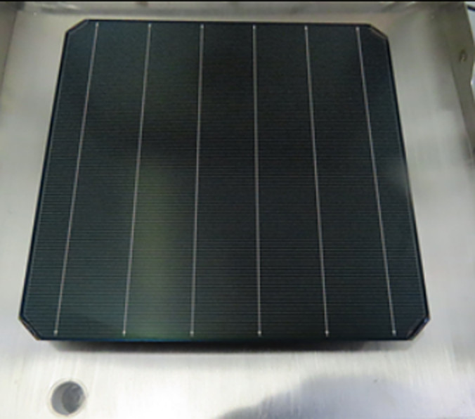
A group of scientists from Chinese solar module maker Longi has described in a new scientific paper the 27.81%-efficient hybrid interdigitated back-contact (HIBC) solar cell it unveiled in April 2025.
At the time, Longi only said the device features the world’s highest efficiency for silicon solar cells, with the result being certified by Germany’s Institute for Solar Energy Research Hamelin (ISFH). “By redesigning both the cell architecture and material systems, we achieved simultaneous breakthroughs in optical management and carrier transport efficiency,” a spokesperson from the company told pv magazine at the time, without providing further details.
In the paper “Silicon solar cells with hybrid back contacts,” which was published last week in nature, Longi’s research team, which also includes its president and founder, Li Zhenguo, explained that the cell is based on passivated tunneling contacts and dielectric passivation layers, while also incorporating both n-type and p-type contacts.
The scientists used a high-resistivity, half-cut M10 wafer with edge passivation, an optimized n-type contact formed through a combined high–low temperature process, an indium tin oxide (ITO) layer to aid lateral transport, and a multilayer stack of aluminum oxide (AlOx) and silicon nitride (SiNx) on the textured front surface to minimize recombination, and an amorphous silicon (a-Si) layer.
They also reduced phosphorus doping in the n-type polycrystalline silicon (n-poly-Si) layer by an order of magnitude to limit dopant diffusion into the wafer. “The high–low temperature process, which combines diffusion and deposition, enables wafer edges to be passivated during fabrication,” they explained, noting that this technique is generally known as in situ passivated edge technology (iPET).
The group also utilized 8-μm deep trenched metal fingers collect holes with selective ITO etched-off to prevent leakage between n-type and p-type contacts. It also enhanced the thicknes of the a-Si layer to ensure adequate coverage of the p–i–n junction and full encapsulation of the n-poly-Si sidewalls. In order to mitigate contact resistivity, the layer was crystallized via pulsed green nanosecond laser to preserve edge passivation.
“Achieving an optimal balance between passivation and conductivity requires careful tuning of the a-Si layer thickness, its optical properties, and laser parameters such as fluence and pulse duration,” the academics emphasized.
The world-record power conversion efficiency of 27.81% was reached on a cell with an active surface of 133.63 cm2. The device also achieved a short-circuit current of 5,698 mA, an open-circuit voltage of 744.9 mV, and a fill factor of 87.55%.
“This performance is driven by integrating advanced techniques, including laser-induced crystallization, in situ edge passivation and optimized surface treatments, which collectively reduce the ideality factor to below 1 at maximum power tracking (MPP), significantly enhancing the fill factor,” the paper notes.
The ideality factor measures how closely the electrical behaviour of a solar cell matches that of an ideal diode, with values tipically ranging from 1 to 2.
Looking ahead, Longi said the new techniques could be readily scaled up for use in heterojunction (HJT) solar cell manufacturing. “The p-type contact shows 50% more resistive loss than the n-type contact, pointing to the need for further improvements in contact resistivity,” the company said.
This content is protected by copyright and may not be reused. If you want to cooperate with us and would like to reuse some of our content, please contact: editors@pv-magazine.com.


By submitting this form you agree to pv magazine using your data for the purposes of publishing your comment.
Your personal data will only be disclosed or otherwise transmitted to third parties for the purposes of spam filtering or if this is necessary for technical maintenance of the website. Any other transfer to third parties will not take place unless this is justified on the basis of applicable data protection regulations or if pv magazine is legally obliged to do so.
You may revoke this consent at any time with effect for the future, in which case your personal data will be deleted immediately. Otherwise, your data will be deleted if pv magazine has processed your request or the purpose of data storage is fulfilled.
Further information on data privacy can be found in our Data Protection Policy.