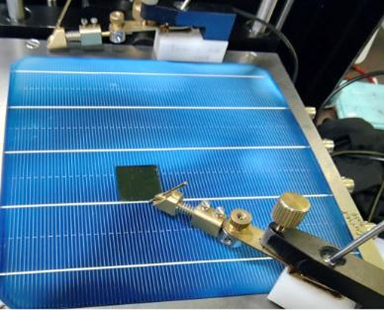
Researchers at the Indian Institute of Technology Bombay have fabricated an inverted low-bandgap perovskite solar cell for applications in four-terminal (4T) perovskite-silicon tandem solar cells.
Inverted perovskite cells have a device structure known as “p-i-n”, in which hole-selective contact “p” is at the bottom of an intrinsic perovskite layer “i” with electron transport layer “n” at the top. Conventional halide perovskite cells have the same structure but reversed – an “n-i-p” layout.
In the conventional n-i-p architecture, the solar cell is illuminated through the electron-transport layer (ETL) side; in the p-i-n structure, it is illuminated through the hole‐transport layer (HTL) surface.
“We optimized a p-i-n opaque perovskite solar cell by gauging the thickness of passivating aluminum oxide (Al2O3) interlayer deposited via atomic layer deposition (ALD),” the research’s corresponding author, Dinesh Kabra, told pv magazine. “We used the Al2O3 nanoparticle interlayer for passivation of perovskite and charge buckminsterfullerene (C60) transport layer interfaces. Al2O3 layer deposition via the ALD technique has shown great potential in the passivation of active layers as well as complete device stack encapsulation.”
The scientists designed the cell with a substrate made of glass and indium tin oxide (ITO), a hole transport layer (HTL) made of a phosphonic acid called methyl-substituted carbazole (Me-4PACz), a perovskite absorber with an energy bandgap of 1.67 eV, the Al2O3 interlayer, the C60 ETL, a bathocuproine (BCP) buffer layer, and a silver (Ag) metal contact.
They used an “optimized” 3 nm-think Al2O3 interlayer, which reportedly helped increase the cell efficiency from 17.09% to 19.16% and the fill factor from 71.44% to 77.36% in comparison with a reference cell without the Al2O3 interlayer.
With this configuration, the research group built a cell with an active area of 0.175 cm2 and an efficiency of 18.77%, as well as a device with an active area of 1.08 cm2 and an efficiency of 16.92%.
Both devices were then integrated into a 4T perovskite-silicon tandem cell with a bottom silicon device with a 25.5% efficiency, an open-circuit voltage of 0.720 V, a short-circuit current density of 4209 mA/cm2, and a fill factor of 84.15%.
Tested under standard conditions, the tandem cell with the 0.175 cm2 top perovskite device achieved an efficiency of 29.14%, while the tandem cell using the 1.08 cm2 top cell reached an efficiency of 26.86%.
“We successfully demonstrated 4-T perovskite-silicon tandem solar cells with efficiency exceeding 26 % over 1 cm2 active area,” said Kabra. “There is a potential for further improvement in the performance of the tandem cells by incorporating an optical coupler between the top and bottom cells which can enhance near-infrared (NIR) transmission.
The cell was described in detail in the study “Optimization of Near Infrared Transparent p-i-n Perovskite Solar Cells with Active Area >1 cm2 for Four-Terminal Perovskite/Si Tandem Solar Cells,” published in RRL Solar.
This content is protected by copyright and may not be reused. If you want to cooperate with us and would like to reuse some of our content, please contact: editors@pv-magazine.com.


By submitting this form you agree to pv magazine using your data for the purposes of publishing your comment.
Your personal data will only be disclosed or otherwise transmitted to third parties for the purposes of spam filtering or if this is necessary for technical maintenance of the website. Any other transfer to third parties will not take place unless this is justified on the basis of applicable data protection regulations or if pv magazine is legally obliged to do so.
You may revoke this consent at any time with effect for the future, in which case your personal data will be deleted immediately. Otherwise, your data will be deleted if pv magazine has processed your request or the purpose of data storage is fulfilled.
Further information on data privacy can be found in our Data Protection Policy.